晶振无信号输出,系统无反应英文版
NO Signal Output from the Crystal
1-1.
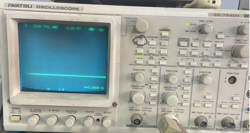
Please measure the signal output by two terminals of the crystal using Oscilloscope or Frequency Counter. If there is no signal output, please follow step 1-1 to step 1-4 to execute the examination. If there is signal output from out- terminal of the crystal ( Xout), but no signal output from the interminal (Xin), please check the crystal following step1-5 to step 1-6.
1-2.
Please uninstall the crystal and test its frequency and load capacitance to see whether they vibrate and meet your specifications using a professional testing machine. You can also send it to your supplier to have them test it for you.
1-3.
If any of the following situations happen, the crystal doesn’t vibrate, its load capacitance doesn’t match your specification,or there is a huge gap between current frequency and your targeted frequency, please send the crystal to your supplier to conduct Quality Analysis. If the frequency and load capacitance meet your specifications, we will need to conduct Equivalent Circuit Test.
1-4.
Equivalent Circuit Test
1-4-1.
Generally, the oscillation circuit of Microprocessor derives from Colpitts circuit showing below:
Picture 1
Cd and Cg are external load capacitances, which have been built in the chip set. (Please refer to the Specifications of the chip set) Rf is the feedback resistance with200KΩ~1MΩ. It’s built in the chip set generally.
Rd is the Limit Resistor with 470Ω~1KΩ. This resistance is not necessary for common circuit but only for circuits having high power supply.
1-4-2.
A stable oscillation circuit requires a negative resistance and its value should be at least five times of the crystal resistance. It can be written as |-R| > 5 Rr.
For example, to acquire a stable oscillation circuit, the value of negative resistance of the IC must be under –200Ω when the value of the crystal resistance is 40Ω.
1-4-3.
“Negative resistance” is the yardstick to evaluate the quality of an oscillation circuit. Under some circumstances such as aging, thermal change, voltage change, and etc., the circuit might not oscillate if the value of “ Q” is low. Thus, it’s very important to measure the negative resistance (-R )following the instructions below:
(1) Connect the resistance (R) with the crystal in series
(2) Adjust the value of R from the start point to the stop point of the oscillation.
(3) Measure the value of R during oscillating.
(4) You will be able to obtain the value of negative resistance, |–R| = R + Rr, and Rr = crystal resistance.
P.S. the stray capacitance of the connected circuit might affect measured values.
1-4-4.
If the parameters of the crystal are normal but it’s not working steadily within the oscillation circuit, we will have to find out whether the resistance value of the IC is too low to drive the circuit. If that’s the case, we have three methods to improve such situation:
Lower the value of external capacitance(Cd and Cg), and adopt other crystal with lower load capacitance (CL).
Adopt a crystal with lower resistance (Rr).
Use the design of unequal values of Cd and Cg. We can increase the load capacitance of Cd (Xout) and decrease the load capacitance of Cg(Xin) to raise the output of waveform amplitude from Xin which will be used in its back-end circuit.
1-5.
When there is signal output from Xout but not Xin, it represents the case that the power consumption of the rear electrode Backend Circuit is extremely huge. We can add a buffer between the output of the circuit and its rear electrode to drive the back-end Circuit.
1-6.
Except the method of 1-5 mentioned above, you can also follow the three methods in step 1-4-4. Please contact the field application engineers of crystal or IC manufacturers for further assistance, if your problem can’t be solved.
02. System is not fun ctioning because of no adequate output waveform amplitude from the crystal ?
2-1.
Please measure the signals from the two terminals of the crystal using Oscilloscope or Frequency Counter, if the Frequency is not within the specification and it’s output waveform amplitude is not adequate (for example, over+/- 200ppm), please follow step 2-3 to step 2-5.
2-2.
The formula for Capacitances versus Frequency is as following:
FL = FR * ( 1 + C1 / 2 * ( C0 + CL) ) where
The curve represents the variation of capacitance changes versus variation of frequency changes ( Frequency pullability):
If the frequency measured by Frequency Counter is higher than the targeted frequency, we should increase the value of capacitances (CL, or Cd & Cg ) to lower the frequency to the targeted frequency, vice versa.
Please check whether the waveform amplitude is improved or not after we adjust the frequency. If it’s improved, that indicates the case that the original design of the circuit is not tuned to the best resonant point for the crystal. The crystal should function normally after the resonant point is adjusted.
2-3.
If the waveform amplitude is not improved even the frequency is pretty much close to the targeted frequency, we can improve it using three methods below:
Method 1: Lower the value of external capacitance (Cd, and Cg) , and adopt crystal with lower load apacitance (CL).
Method 2: Adopt the crystal with lower resistance(Rr).
Method 3: Use the design of unequal values of Cd and Cg.
We can increase the load capacitance of Cd (Xout) and decrease the load capacitance of Cg(Xin) to raise the output of waveform amplitude from Xin which will be used in its back-end Circuit.
We suggest that you use above methods to save costs and assure safety.
2-4.
Please use the Frequency Counter to measuring the crystal to ensure that the adjusted frequency still meets original specification after the waveform amplitude has been improved. If the frequency doesn’t meet the specification, please adopt a crystal with suitable CL value according to your targeted frequency.
2-5.
Please adopt a crystal with lower CL if the frequency is much higher than the targeted frequency, vice versa.
03. System is not functioning due to high deviation of output frequency ?
3-1.
We can improve the problem that deviation of frequency output is over the limit by following methods:
Adjust the values of external capacitance, Cd & Cg.
If the frequency measured by Frequency Counter is higher than targeted frequency, we should increase the external capacitance, CL ( or the values of Cd & Cg ), to lower the frequency to our targeted frequency, vice versa.
Adopt a crystal with different value of capacitance(CL).
Adopt a crystal with lower capacitance if the frequency is much higher than the targeted frequency, vice versa.
3-2.
Please check whether the waveform amplitude is normal or not using Oscilloscope, after the correct capacitance is adopted and the frequency is adjusted to target. Under the situation that the waveform amplitude is shrunk due to adding external capacitances, please use method 2 to adjust the frequency ( lower external capacitances and adopt a crystal with lower capacitance).
了解更多晶振相关资讯,请点击晶诺威官网以下链接:
- 时钟晶振32.768KHz的原理和应用
- 晶振32.768KHz不起振原因及解决方案
- 晶振停振的原因
- 晶振停振的原因及解决方法
- 切不可忽视无源晶振旁边电容的重要作用
- 晶振的负载电容与外接电容的区别与关系
- 哪些因素会破坏晶振?
- 晶振在什么情况下会被烧坏?
- 晶振不起振的原因分析和解决方案
- 超声波封装会把晶振破坏了吗
- 晶振振荡电路中负性阻抗到底是什么?
- 你对晶振的激励功率了解有多少?
- 怎么判断晶振失效了又怎么解决?
- 晶振被误判不良八种常见案例归纳
- 影响晶振起振异常的主要原因有哪些?
- 如何判断晶振是否起振?晶振不起振该怎么办?
- 晶振不起振造成整机不上电问题分析
- 大量晶振不起振造成整机不上电原因分析
- 无源晶振工作原理及起振条件介绍


