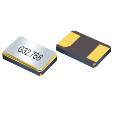
晶体振荡器/Oscillator性能和术语(英文版)
Nominal Frequency: The center or nominal output of a crystal oscillator.
Frequency Tolerance: The deviation from the nominal frequency in terms of parts per million (PPM) at room temperature. (25°C ±5°C)
Frequency Range: The frequency band that the oscillator type or model can be offered.
Frequency Stability: The maximum allowable frequency deviation compared to the measured frequency at 25°C over the temperature window, i.e. 0°C to +70°C. The typical stability for clock oscillators is ±0.01% (±100PPM).
Operating Temperature: Temperature range within which output frequency and other electrical, environmental characteristics meet the specifications.
Aging: The relative frequency change over a certain period of time. Typically aging for clock oscillators is ±5PPM over 1 year maximum.
Storage Temperature: The temperature range within which the unit is safely stored without damaging or changing the performance of the unit.
Supply Voltage: The maximum voltage which can safely be applied to the VCC terminal with respect to ground.
Input Voltage (VIN): The maximum voltage which can be safely applied to any input terminal of the oscillator.
Output HIGH Voltage (VOH): The minimum voltage at an output of the oscillator under proper loading.
Output LOW Voltage (VIH): The maximum voltage to guarantee threshold trigger at the input of the oscillator.
Supply Current: The Current flowing into Vcc terminal with respect to ground. Typically supply current is measured without load.
Symmetry of Duty Cycle: The symmetry of the output waveform at the specified level (at 1.4 V for TTL, at 1/2 Vcc for HCMOS, or 1/2 waveform peak level for ECL).
Rise Time (TR): Waveform rise time from Low to High transition measured at the specified level (20% to 80% for HCMOS, ECL and 0.4 V to 2.4 V for TTL).
Fall Time (TF): The waveform fall time from High to Low transition, measured at the specified level (80% to 20% for the HCMOS, ECL and 2.4 V to 0.4 V for TTL).
Output Load: The maximum load that the different families of oscillators can drive is defined as the output load driving capability. The load driving capability (fan-out) of each family of oscillators is specified in terms of the number of gates an oscillator can drive.
Jitter (short-term stability): The modulation in phase or frequency of the oscillator output.
HCMOS/TTL Compatible: The oscillator is designed with ACMOS logic with driving capability of TTL and HCMOS loads while maintaining minimum logic High of HCMOS.
Tri-State Enable: When the input is left OPEN or tied to logic “1” the normal oscillation occurs. When the input is grounded (tied to logic “0”, the output is HIGH IMPEDANCE state. The input has an internal pull-up resistor thus allowing the input to be left open.
Output Logic: The output of an oscillator is designed to meet various specified logic’s such as TTL, HCMOS, ECL, Sine, Clipped-Sine (DC cut).
Harmonic Distortion: The non-linear distortion due to unwanted harmonic spectrum component related with target signal frequency. Each harmonic component is the ratio of electric power against desired signal output electric power and is expressed in terms of dbc, i.e. -20 dBc. Harmonic distortion specification is important especially in sine output when a clean and less distorted signal is required.
Dual and Multiple Outputs: More than one signal is capable of being generated from a single oscillator. The signals may be related (usually a multiple or divisor of the signal produced by a single crystal).
Start-Up Time: The start up time of an oscillator is defined as the time an oscillator takes to reach its specified RF output amplitude.


