Jitter
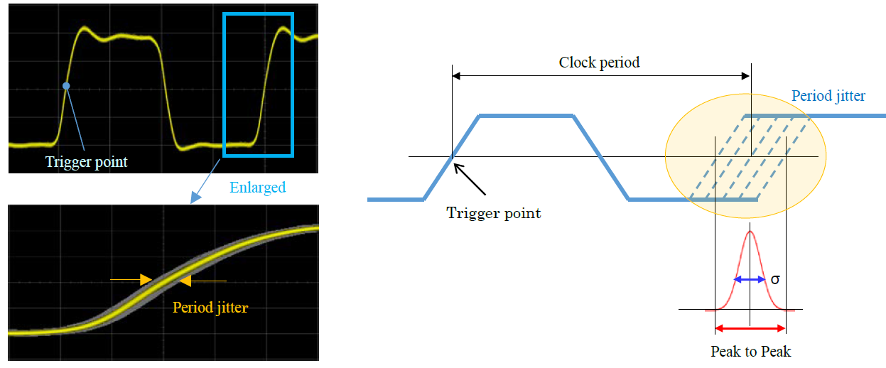
Jitter expresses a drift from the ideal position of the clock edge occurring as the result of the fluctuation of the clock signal waveform in the direction of the time axis.
The output voltage waveform of a crystal oscillator, as shown in the illustration, shows a certain fluctuation range from the position at which the waveform should be originally located in the edge section separated by one period from the trigger point. This fluctuation is called period jitter because it corresponds to the time variation of one period of the clock.
This fluctuation is generally expressed in an RMS or peak-to-peak value in the histogram. Three kinds of unit, rad, second, and unit interval (UI), are available to express a fluctuation. In most cases, however, the unit of second is generally used.
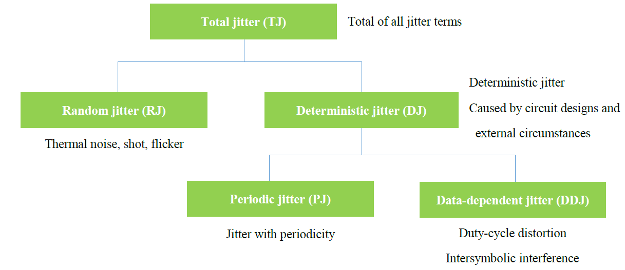
Jitter is roughly classified into random jitter (RJ) and deterministic jitter (DJ) according to the cause of its occurrence.
RJ occurs spontaneously from thermal or shot noise in semiconductor devices. Since RJ occurs as the result of accumulation of a number of minute noise generation processes, its shape of distribution approximates a normal distribution.
On the other hand, DJ is produced by various factors with regularity, such as circuit designs, electromagnetic induction and externally induced factors, being classified into periodic jitter (PJ) and data-dependent jitter (DDJ) according to the cause of its occurrence. The width of variation of its distribution has a characteristic provided with a border that can be expressed by a part sandwiched between RJ on both sides. A specific cause of occurrence that is not random exists, and the drift of the edge is not a random dispersion but a deterministic (predictable) jitter component. Combined together, RJ and DJ are called total jitter (TJ).
A crystal oscillator in which the output frequency is directly produced without using a PLL circuit has almost no DJ component, virtually having an RJ component only.

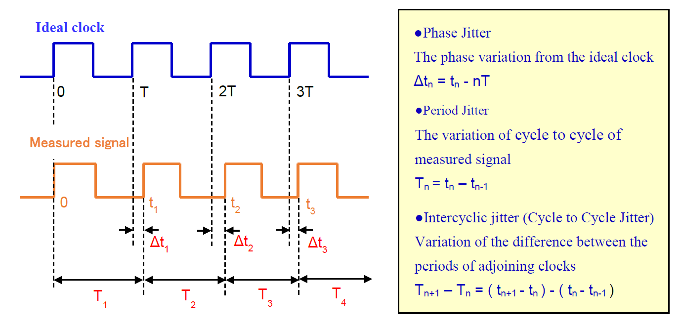
Depending on how the jitter timing is defined, jitter is classified into phase jitter, period jitter, and intercyclic jitter. Phase jitter is an accumulation of the difference between the ideal clock of the clock edge and the measured signal, and it is called long-term jitter or accumulated jitter depending in the case. Period jitter expresses the variation in a clock period and intercyclic jitter the variation in the difference between the periods of adjoining clocks.
Phase noise and phase jitter
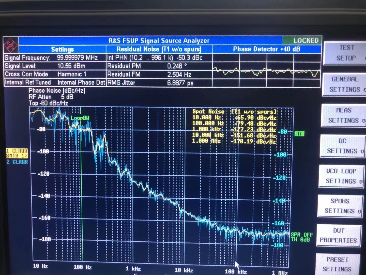
Phase noise refers to the power spectrum density of phase fluctuation, providing a measure showing the purity of a signal.
Phase noise is expressed by the frequency components at the location separated by a certain magnitude from the center frequency (the offset frequency), and the smaller the noise value is, the better the signal is considered to be because of the presence of fewer noise components. Phase noise is usually expressed by normalizing noise in the neighborhood of the single sideband with reference to the carrier electric power.
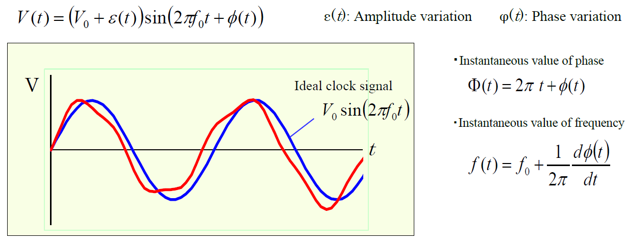
A signal waveform with phase noise V (t) is expressed below in the form of a phase term of an ideal sinusoidal wave with the addition of phase variation Φ (t). The phase noise and the phase jitter are given by the phase variations Φ (t) obtained in the frequency domain and in the time domain.
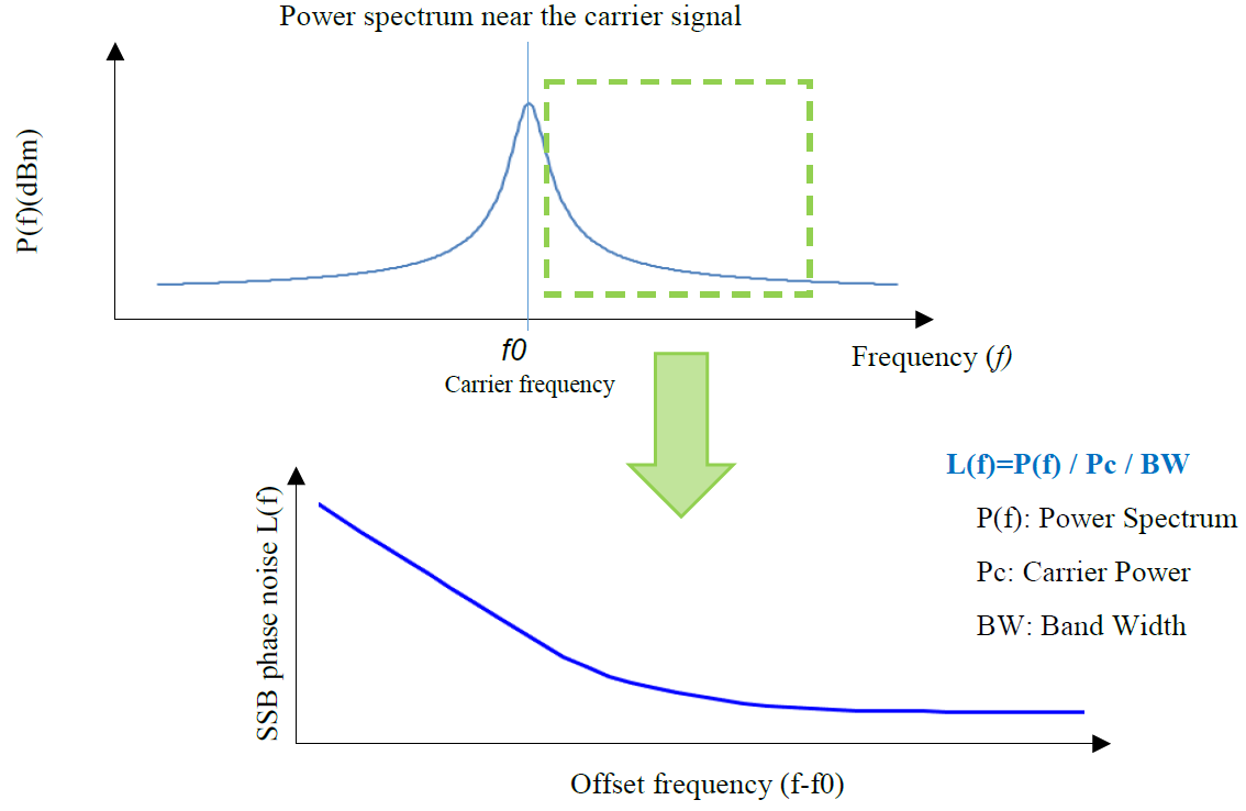
Phase noise is expressed in the frequency domain of the phase variation Φ (t), being defined by the power spectrum density SΦ. In practice, single sideband (SSB) phase noise L (f) expressed in the single sideband is usually used, with the ratio of the carrier signal to the total electric power being expressed in dBc/Hz on the horizontal axis indicating the offset from the carrier frequency.
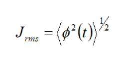
On the other hand, phase jitter is an index of noise in which the phase variation is expressed on the time axis; it can be said to be the function Φ (t) itself. The RMS value of phase jitter is given by the root mean square of Φ (t) as shown below:
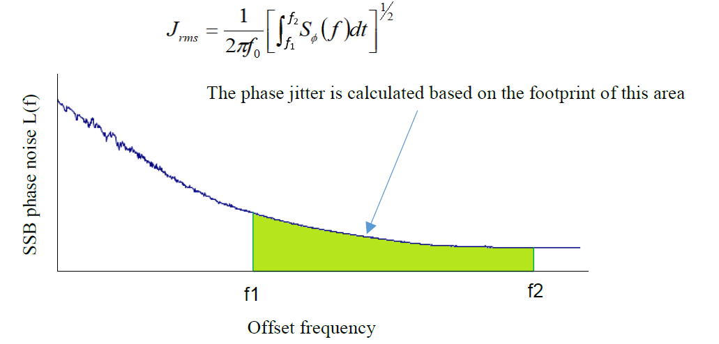
Measuring Φ (t) exactly in the time domain is extremely difficult. However, a convenient method which can be used is first measuring the phase noise and then converting it into the phase jitter according to the following method.
A relationship as shown below approximately holds between the power spectrum density of phase variation SΦ and the SSB phase noise L (f) evaluated in a single sideband:

Under this condition, the phase jitter can be obtained by integrating the measured value of phase noise SΦ between the interval of the designated offset band width.
To obtain clock signals excellent in noise performance
The main part of phase noise in a crystal oscillator is determined by the Q value and signal level of the crystal and the noise performance of the oscillation circuit. In improving the phase noise performance near the carrier frequency of phase noise, the Q value of the crystal plays a particularly important role.
The higher the signal level is, the lower the phase noise level becomes regardless of the offset frequency. Phase noise can be lowered by setting the signal level at as high a value as the system allows. However, the upper level of excitation applicable to a crystal is limited. An excessively high excitation level may cause unnecessary oscillation modes to occur, with the oscillation becoming abnormal.
Overtones help secure high Q values and hence are effective near the offset value. However, you should be careful about overtones because they cause the resistance loss in the crystal and oscillation circuit to increase and also because operating at a highly excited level allows the frequency to fluctuate greatly and thereby to degrade the frequency purity.
In addition, greater electric power causes the frequency fluctuation to increase due to the non-linearity of the crystal, with operation at an excessive excitation level likely to cause deterioration in the phase noise. Selecting semiconductor devices with excellent noise performance is important. The offset frequency of flicker noise affects the frequency zone from the vicinity of the carrier frequency to the vicinity of intermediate frequencies of approximately 10 kHz, while thermal noise affects the entire offset zone in the same way as the signal levels do.
To obtain favorable phase noise
![]() Secure a favorable Q value of the oscillation circuit.
Secure a favorable Q value of the oscillation circuit.
Use a crystal with a high Q value, and lower the resistance loss of the oscillation circuit to obtain Q higher in the oscillation loop.
![]() Minimize the device noise.
Minimize the device noise.
Select a device characterized by minimal values in noise figure (NF), and flicker corner frequency (Fc) to minimize thermal noise, shot noise, and flicker noise from the semiconductor device.
![]() Do not use a frequency multiplication scheme using a PLL circuit because it causes the degradation of phase noise.
Do not use a frequency multiplication scheme using a PLL circuit because it causes the degradation of phase noise.
![]() Enhance the drive level of the oscillator circuit as high as allowed.
Enhance the drive level of the oscillator circuit as high as allowed.
![]() Since the noise characteristic is a relative value of the signal level to the noise power, the higher the signal level is, the more favorable the noise characteristic is. This is, however, on condition that the crystal be used in a domain in which its drive level characteristic is flat.
Since the noise characteristic is a relative value of the signal level to the noise power, the higher the signal level is, the more favorable the noise characteristic is. This is, however, on condition that the crystal be used in a domain in which its drive level characteristic is flat.
![]() Overtones provide a high Q value, being useful in the vicinity of the offset. Note, however, pay attention to the degradation of phase noise by the fluctuation of frequency as that overtones allow the resistance loss in the crystal and the oscillation circuit to grow and that the operation at a higher drive level increases the frequency fluctuation that leads to the deterioration of the signal purity.
Overtones provide a high Q value, being useful in the vicinity of the offset. Note, however, pay attention to the degradation of phase noise by the fluctuation of frequency as that overtones allow the resistance loss in the crystal and the oscillation circuit to grow and that the operation at a higher drive level increases the frequency fluctuation that leads to the deterioration of the signal purity.
![]() Restrict noise from the power supply by placing bypass capacitors in the shortest distances to the power supply and the ground terminal.
Restrict noise from the power supply by placing bypass capacitors in the shortest distances to the power supply and the ground terminal.
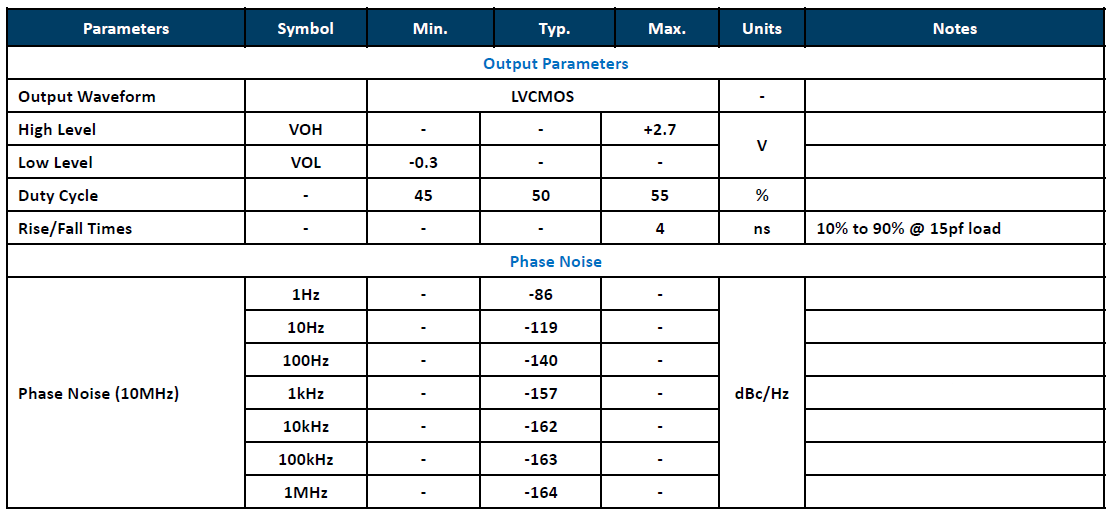
(Electrical Specifications for OCXO 10MHz)
Our products are extensively utilized in various fields such as 5G networks,data centers,telecommunications,power supply,audiophile markets, satellite communications and timing,monitoring systems, base stations,security,radar technology, marine exploration,meteorological observation, rail transportation, medical equipment, and instrumentation.
拓展阅读:Phase noise相位噪声、Jitter抖动和Allan variance艾伦方差
1、相位噪声(Phase noise)
在射频和微波电子学中,相位噪声通常是查看和分析噪声的方法。具有低相位噪声频率源至关重要,因为相位噪声限制了确定振荡器当前状态和可预测性的能力。随着时间的推移,具有良好的频率精度是件好事,但信号的纯度也很重要。
较差的相位噪声限制了通信系统中可以传输和接收的数据量,并干扰了任何通信系统中可用带宽的最有效使用。传统上,在任何模拟、射频或微波应用中,工程师都喜欢在频域中处理相位噪声。
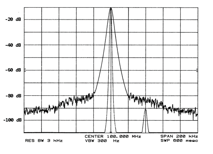
从直观的角度来看,相位噪声可能是可视化信号纯度的最佳方式。如果有一个 100 MHz 的晶体振荡器或其他频率信号,那么希望信号的所有能量都精确到 100 MHz。当在频率分析仪上查看时,它甚至可以显示最佳频率源的输出功率,虽然大部分功率在 100 MHz,但也发现一些功率位于非常接近载波 (100 MHz) 的频率上。离载波越远,噪音就越小。精密石英晶体振荡器实际上是最好的低噪声源,因为石英具有最高的“Q”或品质因数。但在现实世界中,没有一个频率源是完美的。任何给定偏移(与载波的距离)的噪声量均以 dBc/Hz 为单位。
请记住,对于晶体振荡器,相位噪声很低。dBc/Hz 刻度是对数的,因此一个好的晶体振荡器的相位噪声,即使在与载波最近的偏移处(如 10 Hz)也可能约为 -95 dBc/Hz,与载波频率本身的能量密度相比,这是非常非常低的,而 1 MHz 和远离载波的相位本底可能低至 -174 dBc/Hz。
2、抖动 (Jitter)
相比之下,在电信行业,传统上使用抖动在时域中分析噪声。在本质上是数字的电信中,抖动是周期性信号与真实周期性的偏差。相位噪声分析的是频域中信号的纯度,而抖动分析的是所研究的方波信号中每个周期的时序精度。
在电信和其他数字应用中,低抖动对于最大限度地降低误码率 (BER) 非常重要。BER 是衡量数字系统中在给定时间段内将错过多少个运行周期的指标。显然,错过的周期意味着错过或损坏的数据。
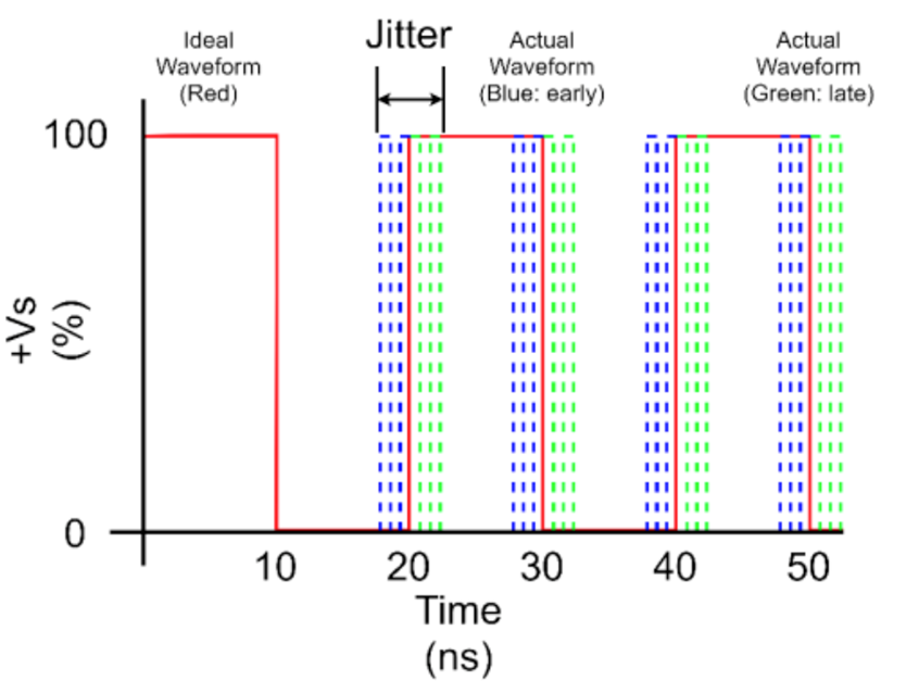
一个完美的方波信号在每个周期中都是完全相同的时间段。抖动是衡量数字定时信号接近此定时完美的程度的指标。由于主时钟会处理任何更短或更接近的噪声,因此可以并且以多种不同方式测量和表征的抖动被视为远离载波频率的 12 KHz 至 20 MHz 的所有相位抖动的积分。这一传统沿用至今,至今仍是指定和测量大多数抖动的方式。
3、艾伦方差 (Allan variance)
Allan 方差是一种统计方法,可以对短期稳定性进行有意义的表征。使用中有一些不同的修改,也许最常见的是 Allan Deviation 或 ADEV。虽然非常接近的相位噪声是检查信号短期稳定性和纯度的有用技术,但一旦真正靠近载波,例如距离载波一秒甚至更近,几乎不可能以可重复的方式准确和精确地测量单个的相位噪声。因此,Allan Deviation 涉及进行许多此类测量,然后对数据集进行统计分析,以有意义地表示信号的非常短期的稳定性。


