(Layout issues of crystal oscillators)
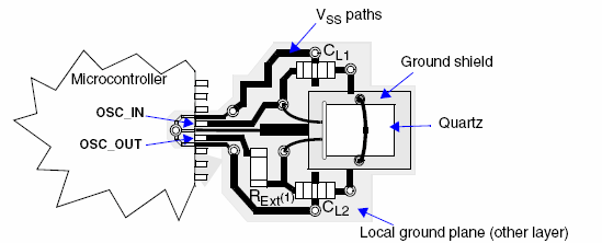
Good layout practices are fundamental to the correct operation and reliability of the oscillator. It is critical to locate the oscillator’s components very close to the XTAL and EXTAL pins to minimize routing distances. Long traces in the oscillator circuit are a very common source of problems. Don’t route other signals across the oscillator circuit, and make sure power and high-frequency traces are routed as far away as possible to avoid crosstalk and noise coupling. Power supply decoupling capacitors should be located very close to the microcontroller’s power pins.
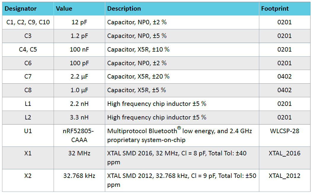
Avoid the use of vias; if the routing becomes very complex, it is much better to use 0 Ω resistors as bridges to go over other signals. Vias in the oscillator circuit should only be used for connections to the ground plane. Don’t share ground connections; instead, make a separate connection to ground for each component that requires grounding. If possible, place multiple vias in parallel for each connection to the ground plane. Especially in the Colpitts configuration, the oscillator is very sensitive to capacitance in parallel with the crystal or resonator. Therefore, the layout must be designed to minimize stray capacitance across the crystal or resonator. For example, in the Colpitts configuration, it’s possible to remove the ground plane from all layers under the EXTAL trace and to leave considerable spacing from the EXTAL trace to all other traces and planes. When stray capacitance appears across capacitors C1 and C2, they should be resized to compensate for this added capacitance. Be sure to take into account both printed circuit board (PCB) and pin capacitance.
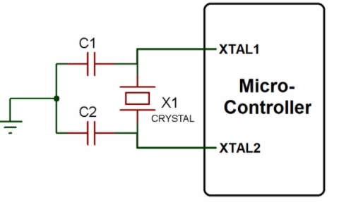
The use of high-quality components in the oscillator circuit is equally important to achieve correct and reliable operation. The use of low-inductance resistors, such as carbon composition resistors, is recommended. Capacitors should be high-quality capacitors with very low ESR, designed for use in high-frequency applications (i.e., NP0 and COG). If a resonator is used, it is critical to choose a very high-quality resonator. Remember that poor layout practices (like long traces) can also contribute to EMC susceptibility and unintentional electromagnetic radiation.
Other Problems
Other common problems include the build up of contaminants on the PCB, hermetic seal fracture, and issues caused by an inadequate soldering process.
PCB contaminants, like flux, humidity, and finger prints, can reduce the impedance between nodes, which in turn can create a number of issues. To overcome this problem, check for contaminant accumulation between the crystal leads and beneath surface mount technology (SMT) devices.
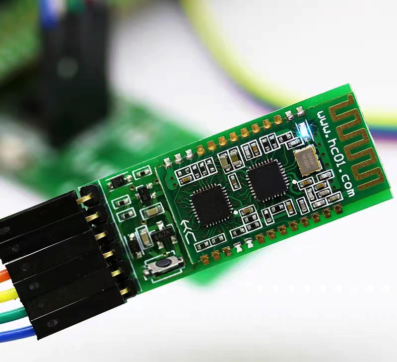
Although uncommon, it is possible for a crystal’s hermetic seal to fracture. This would allow moisture and other contaminants to infiltrate the case, causing sporadic operation or complete failure. To avoid this problem, the crystal should be handled carefully and its case should be adhered to the PCB. A small SMT-type crystal is recommended.
Excessive temperatures or excessive exposure time to high temperatures due to an inappropriate soldering process can also damage the crystal. Make sure the soldering process is compatible with the crystal’s soldering profile.
Conclusion
After following best design practices, if the oscillator doesn’t work properly, it is possible that the selected crystal (or resonator) has poor operating characteristics. In that case, consider choosing a different crystal, but remember that the new crystal’s required external component values will probably be completely different. Selecting an appropriate high-quality crystal is a very important part of the design process and is critical to achieving correct operation and high reliability.
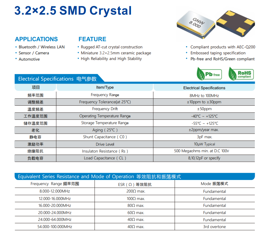
If possible, consult the crystal or resonator manufacturer with respect to the component values. As a domestic crystal manufacturer of over 20 years, Genuway Technology will validate your application board with the crystal or resonator and such an evaluation is strongly recommended.


