(Crystal Oscillator PCB Layout Guidelines for Design)
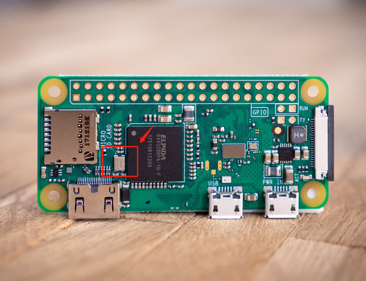
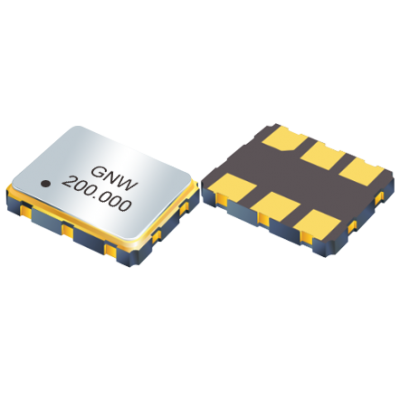
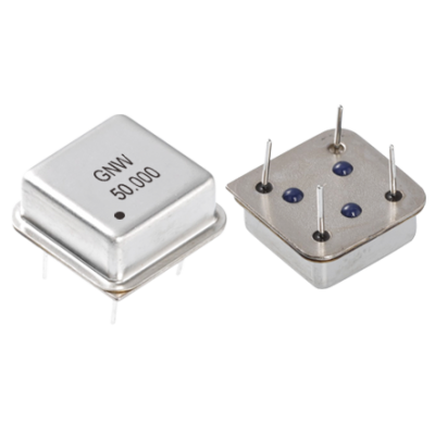
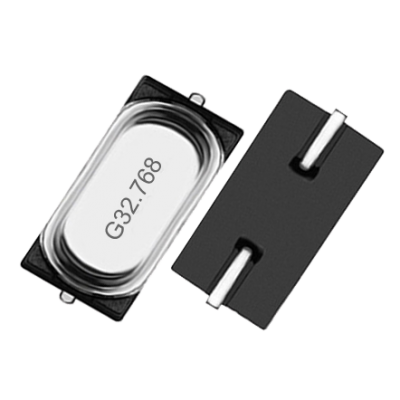
When using a crystal oscillator in your PCB design, remember that it is very EMI sensitive and must be incorporated into the layout carefully. Starting with the component footprint, keep the pad patterns as small as possible to reduce any chance of noise coupling from adjacent signals. Here are some layout considerations for placing and routing the crystal oscillator.
Placement
- Place the crystal oscillator as close as possible to the corresponding input and output pins of the chip.
- Avoid placing the oscillator near high-frequency devices and traces to avoid capacitive coupling.
- Keep the associated capacitors close to the crystal pins.
- Isolate the crystal oscillator for other devices as much as possible.
Routing
Keep the traces connecting the crystal, capacitors, and IC oscillator pins as short and as wide as possible. Not only will this reduce the possibility of noise coupling, but parasitic inductance and resistance as well.
- Avoid right angle bends on these traces, which could change their characteristic impedance leading to reflections.
- Keep differential pair output traces as close together as possible, as well as the same length.
- Keep clock lines and switching signal lines away from the crystal and its connections as far as possible.
- Keep the area under the crystal well-grounded.
These crystal oscillator layout guidelines are similar to the place and route recommendations for analog and power supply circuitry. In general, keep the components connected as close together as possible so that their routed connections can be short, wide, and direct. It is also wise to keep these components on the same layer and use as few vias as possible when routing them together.


